
William G. Spitzer Lecture Series
William G. Spitzer
The Spitzer Lecture was named in honor of physicist William G. Spitzer, who was a member of the USC Viterbi School faculty from 1963-1993.
Renowned in the field of semiconductor physics, Spitzer was the founding chair of the Viterbi School’s original Materials Science Department, and known for his pioneering contributions to the understanding of free carrier absorption, plasmon-phonon coupling, local mode absorption and transport across Schottky barriers. He later served as chair of the Physics Department (1969-72), dean of Natural Sciences (1983-89), and interim provost (1993).
In 1969, Spitzer was awarded the USC Research Award. In 1982, he received the USC Raubenheimer Distinguished Faculty Award and, in 1989, USC bestowed on him its highest honor, the USC Presidential Medallion.
Spitzer’s son, Matthew Spitzer, thanked the Viterbi School and the Mork Family Department of Chemical Engineering and Materials Science for creating the annual Spitzer Lecture as a tribute to his father.
2018
 Professor Philip Kim
Professor of Physics and Applied Physics, Harvard University
"Stacking atomic layers: Quest for new materials and physics"
Friday October 26, 2018, 3:00pm - 4:50pm
Seeley G. Mudd Building (SGM) - 123
Abstract
Modern electronics has been heavily relied on the technology to confine electrons in the interface layers of semiconductors. In recent years, scientists discovered that various atomically thin materials including graphene, a single atomic carbon layer, can be isolated. In these atomically thin materials, quantum physics allows electrons to move only in an effective 2-dimensional (2D) space. By stacking these 2D quantum materials, one can also create atomic-scale heterostructures with a wide variety of electronic and optical properties. I will discuss the creation of new heterostructures based on atomically thin materials and emerging new physics with technological implications therein.
Biography
Professor Philip Kim received his B.S in physics at Seoul National University in 1990 and received his Ph. D. in Applied Physics from Harvard University in 1999. He was Miller Postdoctoral Fellow in Physics from University of California, Berkeley during 1999-2001. In 2002, he joined in Department of Physics at Columbia University as a faculty member. Starting from summer of 2014, he moves to Harvard as Professor of Physics and Professor of Applied Physics.
Professor Kim is a world leading scientist in the area of materials research. His research area is experimental condensed matter physics with an emphasis on physical properties and applications of nanoscale low-dimensional materials. The focus of Prof. Kim’s group research is the mesoscopic investigation of transport phenomena, particularly, electric, thermal and thermoelectrical properties of low dimensional nanoscale materials. These materials include graphene, van der Waals layered materials, carbon nanotubes, and organic and inorganic nanowires. The use of modern state-of-the-art semiconductor device fabrication techniques and the development of new methods of material synthesis/manipulation are essential parts of this research. He has initiated these efforts very successfully, and is continuously making innovations in microscopic experimental tools and methods in order to investigate the electric, thermal/thermoelectric transport properties of the nanoscale materials.
Professor Kim published more than 200 papers in professional journals which are well cited. Many of his papers are published in high impact journals such as Nature, Science and Physical Review Letters. Professor Kim received numerous honors and award including Tomassoni-Chisesi Prizes (2018), Vannevar Bush Faculty Fellowship (2018), Experimental Investigator in Quantum Materials Award, Moore Foundation (2014), Oliver E. Buckley Prize, American Physical Society (2014), IBM Faculty Award (2009), Ho-Am Science Prize (2008); American Physical Society Fellow (2007), Columbia University Distinguished Faculty Award (2007). In addition, He has given more than 400 invited presentations as keynote speaker, plenary speakers, and invited speakers in international and domestic conferences, colloquiums and department seminars.
2012
 Professor Mark A. Reed
Yale University
"Integrated Bioelectronic Systems"
February 2, 2012
Abstract
High performance microelectronic systems and bioelectrochemical systems are both highly developed, complex systems capable of advanced signal processing and computing – yet are fundamentally different at nearly every level (mechanism, device, architecture, etc). A major step in understanding these differences will be the ability to effectively interface between these systems. This talk will review the recent progress, the outstanding scientific challenges, and some exciting potential applications in this rapidly growing new field.
Biography
Prof. Mark A. Reed received his Ph.D. in Physics from Syracuse University in 1983, after which he joined Texas Instruments. In 1990 Mark joined Yale University where he holds the Harold Hodgkinson Chair of Engineering and Applied Science. He was chairman of the Department of Electrical Engineering from 1995 to 2001. He is presently the Associate Director of the Yale Institute for Nanoscience and Quantum Engineering.
Mark’s research activities have included the investigation of electronic transport in nanoscale and mesoscopic systems, artificially structured materials and devices, molecular scale electronic transport, plasmonic transport in nanostructures, and chem/bio nanosensors. Mark is the author of more than 180 professional publications and 6 books, has given over 20 plenary and over 300 invited talks, and holds 25 U.S. and foreign patents on quantum effect, heterojunction, and molecular devices. He is the Editor in Chief of the journal Nanotechnology, an Editor for IEEE Transactions Electron Devices, and holds numerous other editorial and advisory board positions.
Mark has been elected to the Connecticut Academy of Science and Engineering and Who's Who in the World. His awards include; Fortune Magazine “Most Promising Young Scientist” (1990), the Kilby Young Innovator Award (1994), the Fujitsu ISCS Quantum Device Award (2001), the Yale Science and Engineering Association Award for Advancement of Basic and Applied Science (2002), Fellow of the American Physical Society (2003), the IEEE Pioneer Award in Nanotechnology (2007), and Fellow of the Institute of Electrical and Electronics Engineers (2009).
2011
Professor Harry Atwater
California Institute of Technology
"New Photonic Material Designs for Solar Energy Conversion"
Thursday, January 20, 2011
Abstract
Solar energy is currently enjoying substantial growth and investment, owing to worldwide sensitivity to energy security and climate change , and this has spurred basic research on light-matter interactions relevant to solar energy. Professor Atwater will describe approaches to control of light-matter interactions leading to enhanced light-trapping and absorption, as well as increased open circuit voltage and enhanced quantum efficiency in solar photovoltaic structures. Conventionally, photovoltaic cells have a physical thickness comparable to their ‘optical thickness’ for full light absorption and photocarrier current collection. Solar cell design and material synthesis considerations are strongly dictated by this simple optical thickness requirement. Dramatically reducing the absorber layer thickness or volume confers several fundamental and practical benefits, including increased open circuit voltage and conversion efficiency, and also expansion of the scope and quality of absorber materials that are suitable for photovoltaics. He will describe light absorption in thin film and wire array solar cells that demonstrate enhanced absorption compared with conventional photovoltaic cells, and limits to enhanced absorption will be explored. Plasmonics and metamaterials design can also be exploited advantageously in photovoltaics. He will describe design approaches using metallic nanostructures to enhance the radiative emission rate and hence also the photovoltaic material quantum efficiency relative to conventional light-trapping structures. Finally, future design metamaterials for broadband resonant absorption and spectrum-splitting will be discussed.
Biography
Harry Atwater is currently the Howard Hughes Professor and Professor of Applied Physics and Materials Science at the California Institute of Technology. His research interests center around photovoltaics and renewable energy and plasmonics and metamaterials. Atwater and his group have been active in photovoltaics research for more than 20 years. He received his S.B. (1981), S.M. (1983), and Ph.D. (1987) in Electrical Engineering from the Massachusetts Institute of Technology. He is an early pioneer in surface plasmon photonics; he gave the name to the field of plasmonics in 2001. Professor Atwater currently serves as Director of the DOE Energy Frontier Research Center on Light-Matter Interactions in Solar Energy Conversion and was recently named as Director of the Resnick Institute for Science, Energy and Sustainability.
2010
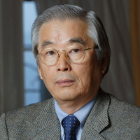 Professor Sumio Iijima
Meijo University
Nagoya, Japan
Challenge to Seeing Atomic Structures of Nano-materials with Electron Microscopy
Monday, March 22, 2010
ABSTRACT
Nanoscience deals with nano-scale structures of materials and therefore controlling the structures is crucial. A typical example of nanostructures is carbon nanotubes and their many unique properties have been investigated theoretically and experimentally, and brought a new concept of materials into condensed matter physics. More importantly, nanoscience is closely related to nanotechnology and thus to industrial applications as we see in many fields of carbon nanotube research. An important issue for nanoscience is characterization of materials. In the case of carbon nanotubes their exact atomic structures are determined by means of electron microscopy, Raman and photoluminescence spectroscopy, etc., where sometimes commercially available instruments are not sufficient and need substantial modification for each particular purpose, where “do it yourself” becomes important. We demonstrate some latest results on structural characterization of carbon nanotubes, graphene, and boron nitride thin films, including “monatomic carbon strings that have been successfully observed in our laboratory.
BIOGRAPHY
Sumio Iijima is a Professor at Meijo University, a Director of the Nano-tube Research Center at AIST and a Senior Research Fellow at NEC, in Japan. After graduating from Tohoku University, he joined Arizona State University where he developed high-resolution transmission electron microscopy (HRTEM) (1970-1982). In 1982 he returned to Japan and joined the NEC Research Laboratories in 1987. In 1991 he discovered carbon nanotubes that have initiated nano-material science and nanotechnology. Professor Iijima has received numerous honors and awards from Italy, Japan, Spain and Switzerland. He is a foreign associate of the National Academy of Science (USA).
TIME AND LOCATION
Monday, March 22, 2010
Seminar at 11:00 a.m.
Ethel Percy Andrus Gerontology Center (GER) Auditorium
A reception will follow in the HEDCO Foundation Building (HED) lobby.
2009

Professor George M. Whitesides
Department of Chemistry and Chemical Biology
Harvard University Cambridge, MA
Simple Bioanalytical Systems
Time and Location
Thursday, February 19, 2009
Seminar at 3:30p.m. SAL - 101
The Scientific Community is Cordially Invited.
Abstract
Simplicity and economy are often the keys to successful technologies. “Simple solutions” is the phrase we apply to the idea of using science to provide easily used solution to a variety of problems in bioanalysis, with a particular focus on problems in developing economies. The requirements for low cost, ruggedness, and independence of infrastructure characteristic of problems in developing economies pose remarkably challenging problems for advanced science and technology—and the area is one that will benefit enormously from new ideas. Successful solutions will also be useful both in developing economies and in the developed world: low cost and simplicity are advantages almost everywhere. The flow of problems, ideas, and solutions stimulated by considering these problems is thus a most interesting two-way street. This talk will discuss this class of problems within the specific context of medical diagnostics (how close can one come to “Zero-cost Diagnostics”?), and with a focus on three technologies: microfluidic systems based on patterned paper, microanalytical systems using magnetic levitation, and simple microfluidics devices for use with simple organisms.
Lecturer's Webpage:
2007
Professor James R. Heath
The California Institute of Technology Department of Chemistry
MC 127-72 Pasadena, CA
Wednesday, February 21, 2007
NanoSystems Biology and New Technologies for in vitro and in vivo Diagnostics of Cancer
Abstract
The emerging world of personalized, preventative, predictive, and participatory (P4) medicine will likely be enabled by the developing field of systems biology. Systems biology and P4 medicine both data driven and, accordingly, both require new tools for making large numbers of measurements rapidly, quantitatively, and inexpensively. Microfluidics, chemical, and nanotechnologies will revolutionize our ability to generate comprehensive data sets that span from individual cells to patients, and will allow us to build multiparameter analysis tools (quantitating genes, proteins, and cells) for achieving an informative in vitro disease diagnosis, as well as in vivo molecular imaging probes for spatially localizing specific diseases. Using cancer as a theme, I will describe the state-of-the-art in terms of network models of human diseases, and I will describe how those models may be harnessed for information that can impact clinical care of cancer. I will then describe a suite of in vitro and in vivo multiparameter diagnostics technologies that we are developing in my lab in concert with other groups, in the context of both near term and far term applications.
About the Speaker
Professor James Heath is the Elizabeth W. Gilloon Professor and Professor of Chemistry at Caltech, Professor of Molecular & Medical Pharmacology at UCLA, and Director of the National Cancer Institute's NanoSystems Biology Cancer Center. Heath received his Ph.D. in Chemistry in 1988 from Rice, where he was the principal student involved in the Nobel Prize–winning discovery of C60 and the fullerenes. He was a Miller Fellow at UC Berkeley from 1988-91, and on the Technical Staff at IBM Watson Labs from 1991-94. In 1994 he joined the faculty at UCLA. He founded the California NanoSystems Institute in 2000 and served as its Director until moving to Caltech. Heath has investigated quantum phase transitions in quantum-dot designed materials, and he has developed architectures, devices, and circuits for molecular electronics. His group has recently been applying their nano/molecular electronics work toward addressing problems in cancer. He has received a number of awards, including a Public Service Commendation from Governor Grey Davis, the Feynman Prize, the Raymond and Beverly Sackler Prize in the Physical Sciences (Israel), and the Spiers Medal from the Royal Society (U.K.)
Materials Science Center
2007
03/05/2007:Facilities Engineering Is It a Necessary Technology? by Kenneth E. Arnold, USC
03/02/2007: Extracellular Electron Transport: Mechanism(s) and Applications, by Ken Nealson Wrigley, USC
02/23/2007: Deformation and Failure of Composite Structures, by Dr. Chiara Bisagni, MIT
02/02/2007: Microscale Flow and Transport Problems arising in Surfactant Rheology, Printing Processes, and Polymer Electrophoresis, by Professor Satish Kumar, University of Minnesota
01/26/2007: Some Experimental Results on Adiabatic Shear Banding, by D. Rittel, Mechanical Engineering Technion (Israel)
01/19/2007: Electrophoresis of Highly Charged Colloids, by Dr. Apratim Chatterji, University of Toronto
01/12/2007: Microbial fuel cell operation for electricity generation, by Zhen He, Washington University
11/03/2006: Is Segregation-induced Grain Boudary Embrittlement a Polymorphous Melting Process? by Dr. Nghi Q. Lam, Argonne National Laboratory
10/20/2006: Research by Neutron Scattering: Tradition and Outlook, by Dr. Gian P. Felcher, Argonne National Laboratory
10/13/2006: The Relationship Between Crystallographic Pitting and Metallic Bonding, by Dr. Scott Lillard, Los Alamos National Laboratory
10/06/2006: Modeling of Materials and Chemistry at Extreme Conditions, by Dr. Sergey Zybin, Caltech
09/28/2006: Ultrafast Biological Dynamics at Atomic Scale, by Dongping Zhong, Ohio State University
09/15/2006: Visible and Infrared spectroscopy of nitride quantum wells and dots, by Dr Matthew Halsall, University of Manchester
09/08/2006: From Electrons To Finite Elements: A Concurrent Multiscale Approach For Metals, by Gang Lu, California State University, Northridge
09/01/2006: Increased Electrode Impedance as a Mechanism of Recording Instability, by Daniel R. Merrill, Alfred E. Mann Foundation for Scientific Research
2006
04/28/2006: Ultra-High Temperature Ceramics for Hypersonic Flight Vehicles, by Jochen Marschall, SRI International
04/21/2006: Processing and Characterization of Nanocrystalline Materials with Interesting Physical Properties, by Amiya K. Mukherjee, UC Davis
04/14/2006: Thermoelectric Materials for Space Power Generation, by Dr. Thierry Caillat, JPL/Caltech
04/07/2006: Scaling Properties of Fracture Surfaces, by Elisabeth Bouchaud, Caltech/CEA-Saclay (France)
03/10/2006: Opportunities in Nanomagnetism, by Samuel Bader, Argonne National Laboratory
02/24/2006: Carbon Nanotubes: The Tall Order, by Professor P. M. Ajayan, RPI
02/17/2006: Phase transitions in polyelectrolytes, polyampholytes and charged colloids, by Prof. A.Z. Panagiotopoulos, Princeton
02/10/2006: Fabrication and Characterization of Nanoscale Hybrid Structures and Devices, by Jia Grace Lu, UC Irvine
02/03/2006: Protein Dynamics At Atomic Scale, by Dongping Zhong, Ohio State
01/27/2006: Electrical Field Enhanced Sintering and Reactions, by Professor Joanna Groza, UC Davis
01/20/2006: NANOMECHANICS: Quantized Motion, Stochastic Resonance & Nanoscale Memory, by Pritiraj Mohanty, Boston University
01/13/2006: From Nature to Engineering: Biotechnology, Biomimetics, and Bio-Inspiration Opens Novel Routes to Metal Oxide Semiconductors, by David J. Kisailus, UCSB
11/18/2005: "Bioengineering of Heart Valves", by Dr. Ivan Vesely, Children's Hospital Los Angeles/USC
11/04/2005: "Behind the scenes at Physical Review Letters or What happens after you click the submit button", by Dr. Donavan Hall, Physical Review Letters
10/28/2005: Hurdles in Nanobiotechnology: A Biologist’s Perspective, by Professor Ram H. Datar, USC
10/21/2005: Electrochemical behavior and corrosion modes of metallic materials used for biomedical applications, by Sannakaisa Virtanen, University of Erlangen-Nuremberg (Germany)
10/19/2005: Nanostructure and reactivity of ultra-thin oxide films on metal and alloy surfaces, by Philippe Marcus, CNRS-ENSCP (France)
09/30/2005: A transferable computational method for atomistic-scale dynamical simulations of chemical reactions, by Professor Adri van Duin, Caltech
09/23/2005: Amazing Nanaochemistry and Nanomechanics at Silicon Carbide Surfaces, by Professor Patrick G. Soukiassian, CEA-Saclay/Universite de Paris-Sud (France)
09/09/2005: Nanotechnology and the Development and Analysis of Energetic Materials, by Professor Richard A. Yetter, Penn State
08/26/2005: The Signficance of Hyperelasticity for Dynamic Fracture, by Professor Markus J. Buehler, Caltech
Published on April 26th, 2017
Last updated on January 31st, 2021